

Okay, so this might be borderline plagiarism. The only difference between the regular Pro Mini and my version is the MCU. I happen to have the MLF package which is about quarter of the size of the normal QFP package on the Pro Mini. The main difference is here that my package has a thermal ground pad, where the QFP has only its leads. This mean that I can’t have any vias unerneath my chip. Okay, I get that let’s get drawing.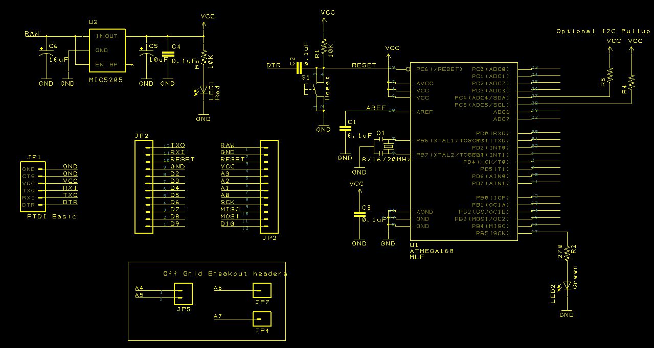
I have not done anything fancy here – I have copied the schematic from the original Pro Mini and ported it to DesignSpark. Then I changed the part numbering so it actually matches the content – if there are 4 resistors, they should be labeled R1, R2, R3 and R4, but that might just be me.
Reset circuit and pinout has not changed since the QFP and the MLF are pin compatible. Now, lets do the routing
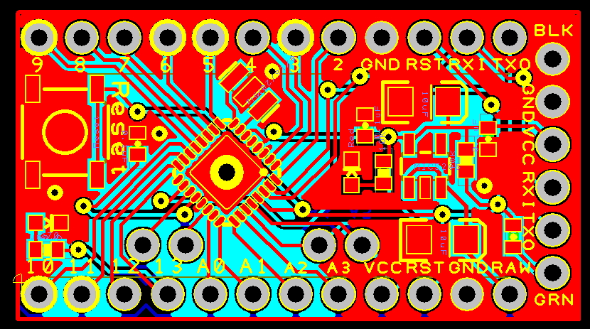 This is the 2nd revision of the board. The first one didn’t have the extra ADC inputs, A6 and A7. The chip has the pins so of course the breakout should be there. I have rerouted the whole board and rearranged the parts so they will fit on the same outline as the original Pro Mini.
One trick I had to pull off was the via for the thermal pad. I don’t have access to a reflow oven (yet) so I made a really large hole through which I can put some solder in when I am done with the board. also, on the ‘original’ pro mini which has the QFP package, there are a few vias under the chip itself. Naturally I had to reroute the wires for those since the thermal pad won’t allow anything to be underneath the chip.
For now, the board files are available here: Arduino Pro Mini Rev. 2 design files